色婷婷精品国产一区二区三区-国产又大又粗又长-99热最新网址-aaa视频-欧美激情自拍-在线h片-国产人妖在线-国产精品爽爽爽-国产黄在线-www.日韩视频-欧美成人免费网站-中文成人无字幕乱码精品区-欧美激情在线看-黄瓜视频色版-日韩av在线播放观看-亚洲春色在线-91大神视频在线播放-精品久久毛片-97无码精品人妻-91激情视频在线-免费h在线观看-看国产黄色片-久草视频2-有码日韩-好吊一二三-永久精品网站-亚洲网中文字幕-国产精品网站入口-女同做爰猛烈叫-很狠撸

企業文化愿景與使命

Solution for Substrate/epitaxial wafer EPD dislocation Inspection

Home / Semiconductor Machine Vision inspection /

Solution for Substrate/epitaxial wafer EPD dislocation Inspection

Solution for Substrate/epitaxial wafer EPD dislocation Inspection

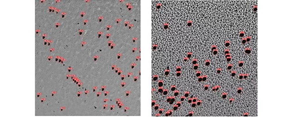
The shape and distribution of dislocation defects in the preparation of semiconductor wafers have a great impact on the performance of electronic components. Due to different doping materials and preparation processes, the dislocation distribution is also different. This solution is mainly aimed at the shape and distribution of wafer dislocations, and is committed to providing data support for wafer material research and improvement of preparation process. It is applicable to 2-inch, 3-inch, 4-inch and 6-inch GaAs substrates.


特色方案
  • Convenient and efficient

    Convenient and efficient surface defect detection equipment for wafers, substrates and epitaxial wafers. Main defects: dislocations, particles, pits, scratches, stains, etc.

  • Improve efficiency and accuracy

    It replaces manual sampling inspection and greatly improves the detection efficiency and accuracy.

  • Data support+automation

    Check the dislocation density, morphology and distribution of the substrate and epitaxial wafer to provide data support for substrate material research, defect traceability, and improvement of preparation process;

    Automatic image acquisition and artificial intelligence analysis tools.

  • High quality service

    Reliable equipment, long trouble free working time, fast response+high-quality after-sales service.

Recommended solution
Substrate EPD testing machine

The shape and distribution of dislocation defects in semiconductor wafer preparation have a significant impact on the performance of electronic components. Due to differences in doping materials and preparation processes, the distribution of dislocations also varies. This device is used to inspect the morphology and distribution of wafer dislocations, providing data support for wafer material research and improving preparation processes. Suitable for 2-inch, 3-inch, 4-inch, and 6-inch gallium arsenide substrates.

View More
Top

Message Board

Message Board
If you are interested in our products and want to know more details, please leave a message here and we will reply to you as soon as possible
Submit

Home

Products

whatsApp